
![]()
Innovation begins here — shaping the future no one has imagined
Ruthenium Wiring: Pioneering Semiconductor
Miniaturization for the AI Era
As generative AI spreads, the performance demands on semiconductors—the brains and memory devices of digital equipment—are increasing rapidly. To enhance integration density, which directly impacts performance, researchers are exploring ways to push beyond current technological limits.
At the forefront of this development, a notable shift is occurring: transistor wiring materials are moving from conventional copper to ruthenium(Ru). Ruthenium supports denser wiring with lower resistivity and faster signal transmission, making it a highly promising alternative for advanced, miniaturized circuits.
Growing demand for miniaturization in the semiconductor industry
The sputtering targets developed and sold by Furuya Metal have the potential to reshape semiconductor manufacturing. This promise is driven by the explosive demand for miniaturization.
The evolution of electronic devices has long relied on the higher integration of “logic semiconductors,” such as CPUs that handle computation and control, and “memory semiconductors,” such as DRAM for data storage.
Higher integration involves packing more transistors into denser arrangements on smaller substrates, enhancing overall performance.
This trend of increasing integration—famously described by Moore’s Law, which states that transistor density roughly doubles every two years—has guided semiconductor development for over half a century.
Today, however, miniaturization technology faces significant challenges. To achieve even higher integration, the wiring width of transistor circuit patterns must continue to shrink, pushing current manufacturing limits.
Over the past two decades, line widths have steadily shrunk—from 130 nm to 90 nm, 45 nm, and now to approximately 10 nm.
However, once line widths drop below 40 nm, copper wiring, long the industry standard, experiences increased resistivity, causing slower signal transmission and a marked decline in electrical efficiency.
In addition, the recent surge in generative AI has pushed semiconductors to deliver performance beyond Moore’s Law, requiring integration densities that now need to double not in two years, but in just four months.
AI and Moore’s Law in comparison

In line with Moore’s Law, transistor density has doubled approximately every two years. However, the performance demanded by AI now doubles in just about four months.
In response, semiconductor manufacturers and equipment makers are re-evaluating designs from multiple angles—including materials, structures, and manufacturing processes—to reduce resistivity. Amid these efforts, ruthenium-based wiring is attracting increasing attention.
To support this trend, Furuya Metal has developed ruthenium sputtering targets, essential for producing such wiring. Ruthenium wiring reduces resistivity and enables three-dimensional structures that support higher integration, making it a promising alternative to copper in future miniaturized circuits.
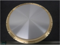
Note: A “target” is the material used in sputtering and other thin-film technologies, which is deposited as a layer onto a substrate. Furuya Metal produces targets from ruthenium and other precious metals using proprietary, advanced processing technologies.
Leveraging world-leading technological strengths
Furuya Metal began focusing on ruthenium sputtering targets for semiconductor wiring in the early 2010s. Even before that, the company had already supplied ruthenium targets for MRAM, a type of memory semiconductor.
As global semiconductor manufacturers invested heavily in next-generation devices, they turned to Furuya Metal—recognized for its expertise in ruthenium handling—to develop sputtering targets for ruthenium wiring.
While basic research on ruthenium wiring began in the early 2000s, by around 2010 no company had yet mass-produced high-quality ruthenium targets for semiconductors. Leveraging its long-standing specialization in iridium and ruthenium and its world-leading share in ruthenium targets for hard disks, Furuya Metal launched development in 2012 of targets for 300 mm wafers using high-purity ruthenium.
Ruthenium’s hardness and brittleness make it extremely difficult to process, and producing high-purity targets at scale was considered highly risky. Furuya Metal overcame these challenges through proprietary technologies, earning strong recognition from semiconductor manufacturers.
The company began shipping its first sputtering targets specifically for ruthenium wiring in semiconductors, taking the first steps toward the practical application of next-generation semiconductors—in close collaboration with global semiconductor manufacturers, equipment makers, and research institutions.
Addressing challenges toward commercialization and mass production
While ruthenium wiring offers significant potential to reduce resistivity as wiring widths shrink, several hurdles remain before its practical application and mass production in next-generation semiconductors can be realized.
To overcome these challenges, semiconductor manufacturers, equipment makers, and research institutions are optimizing film deposition conditions, developing new equipment, and building integrated processes that coordinate with upstream and downstream steps. Furuya Metal supports these efforts by listening closely to each customer’s needs and developing sputtering targets that address their specific challenges.
A key focus of these optimization efforts is cost reduction, the greatest challenge for ruthenium wiring. As one of the rarest precious metals, ruthenium has long been expensive, and recent geopolitical risks—including the COVID-19 pandemic and the war in Ukraine—have further driven up prices.
To address this, Furuya Metal develops customer-tailored products while leveraging its expertise in refining, processing, and high-purification technologies to enhance ruthenium recycling. Through this dual approach, the company aims to reduce costs while maintaining a stable, reliable supply of this critical material.
Challenges
- Ruthenium is difficult to handle and extremely hard to process.
- It is highly rare.
Furuya Metal’s Solutions
- Leverage decades of research on ruthenium to understand its material properties and enable advanced processing.
- Ensure a stable supply through proprietary recycling and high-purification technologies.
Toward mainstream products in the age of AI
Ruthenium sputtering targets for wiring are emerging as one of the most promising next-generation materials for enabling semiconductor miniaturization. They are expected to be gradually adopted in advanced logic semiconductors and, over successive product generations, become mainstream materials in AI-enabled electronic devices.
As industrial machinery, automobiles, home appliances, and social infrastructure become increasingly connected through semiconductor sensors, automation and optimization accelerate. This evolution is driving society into the “age of AI,” laying the foundation for safer, more convenient, and more prosperous living.
Within this major trend, Furuya Metal is dedicated to broadly contributing to society through the widespread adoption of ruthenium wiring. This is made possible by over a decade of expertise in developing sputtering targets, coupled with the advancement of recycling technologies that scale with shipment volumes—achieving a high-level balance of quality and cost.